Building a Big Future from Small Things
Nanotechnology has potential to revolutionize our daily lives and one aspect that makes this technology so promising and effective is its bottom-up approach.
Published October 1, 2002
By Charles M. Lieber
Nanotechnology has gained widespread recognition with the promise of revolutionizing our future through advances in areas ranging from computing, information storage and communications to biotechnology and medicine. How might one field of study produce such dramatic changes?
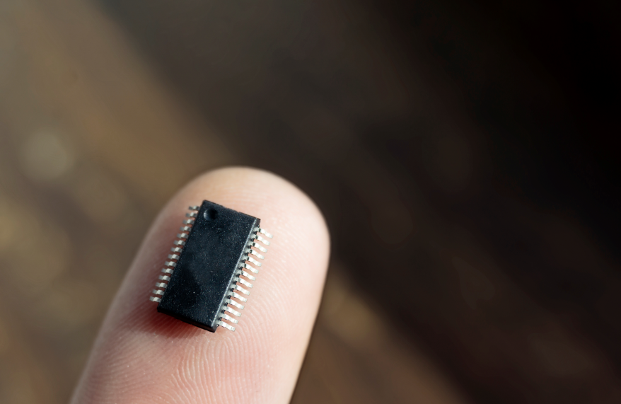
At the most obvious level nanotechnology is focused on the science and technology of miniaturization, which is widely recognized as the driving force for the advances made in the microelectronics industry over the past 30 years. However I believe that miniaturization is just one small component of what makes and will make nanoscale science and technology a revolutionary field. Rather, it is the paradigm shift from top-down manufacturing, which has dominated most areas of technology, to a bottom-up approach.
The bottom-up paradigm can be defined simply as one in which functional devices and systems are assembled from well-defined nanoscale building blocks, much like the way nature uses proteins and other macromolecules to construct complex biological systems. The bottom-up approach has the potential to go far beyond the limits of top-down technology by defining key nanometer-scale metrics through synthesis and subsequent assembly – not by lithography.
Producing Structures with Enhanced and New Functions
Of equal importance, bottom-up assembly offers the potential to produce structures with enhanced and/or completely new function. Unlike conventional top-down fabrication, bottom-up assembly makes it possible to combine materials with distinct chemical composition, structure, size and morphology virtually at will. To implement and exploit the potential power of the bottom-up approach requires that three key areas, which are the focus of our ongoing program at Harvard University, be addressed.
First and foremost, the bottom-up approach requires nanoscale building blocks with precisely controlled and tunable chemical composition, structure, morphology and size, since these characteristics determine their corresponding physical (e.g. electronic) properties. From the standpoint of miniaturization, much emphasis has been placed on the use of molecules as building blocks. However, challenges in establishing reliable electrical contact to molecules has limited the development of realistic schemes for scalable interconnection and integration without having key feature sizes being defined by the conventional lithography used to make interconnects.
My own group’s work has been focused on the nanoscale wires and, in particular, semiconductor nanowires as building blocks. This focus was initially motivated by recognition that the one-dimensional nanostructures represent the smallest morphology structure for efficient routing of information – either in the form of electrical or optical signals. Subsequently, we have shown that nanowires can also exhibit a variety of critical device function, and thus can be exploited as both the wiring and device elements in functional nano-systems.
Control Over Nanowire Properties
Currently, semiconductor nanowires can be rationally synthesized in single crystal form with all key parameters – including chemical composition, diameter and length, and doping/electronic properties – controlled. The control that we have over these nanowire properties has correspondingly enabled a wide range of devices and integration strategies to be pursued. For example, semiconductor nanowires have been assembled into nanoscale field-effect transistors, light-emitting diodes, bipolar junction transistors and complementary inverters – components that potentially can be used to assemble a wide range of powerful nano-systems.
Tightly coupled to the development of our nanowire building blocks have been studies of their fundamental properties. Such measurements are critical for defining their limits as existing or completely new types of device elements. We have developed a new strategy for nanoscale transistors, for example, in which one nanowire serves as the conducting channel and the other crossed nanowire as the gate electrode. Significantly, the three critical device metrics are naturally defined at the nanometer scale in assembled crossed nanowire transistors:
(1) a nanoscale channel width determined by the diameter of the active nanowire;
(2) a nanoscale channel length defined by the crossed gate nanowire diameter; and
(3) a nanoscale gate dielectric thickness determined by the nanowire surface oxide.
These distinct nanoscale metrics lead to greatly improved device characteristics such as high gain, high speed and low power dissipation. Moreover, this new approach has enabled highly integrated nanocircuits to be defined by assembly.
Hierarchical Assembly Methods
Second and central to the bottom-up concept has been the development of hierarchical assembly methods that can organize building blocks into integrated structures. Obtaining highly integrated NWs circuits requires techniques to align and assemble them into regular arrays with controlled orientation and spatial location. We have shown that fluidics, in which solutions of nanowires directed in channels over a substrate surface, is a powerful and scalable approach for assembly on multiple-length scales.
In this method, sequential “layers” of different nanowires can be deposited in parallel, crossed and more complex architectures to build up functional systems. In addition, the readily accessible crossed nanowire matrix represents an ideal configuration since the critical device dimension is defined by the nanoscale cross point, and the crossed configuration is a naturally scalable architecture that can enable massive system integration.
Third, combining the advances in nanowire building block synthesis, understanding of fundamental device properties and development of well-defined assembly strategies has allowed us to move well beyond the limit of single devices and begin to tackle the challenging and exciting world of integrated nano-systems. Significantly, high-yield assembly of crossed nanowire structures containing multiple active cross points has led to the bottom-up organization of OR, AND, and NOR logic gates, where the key integration did not depend on lithography. Moreover, we have shown that these nano-logic gates can be interconnected to form circuits and, thereby, carry out primitive computation.
Tremendous Excitement in the Field
These and related advances have created tremendous excitement in the nanotechnology field. But I believe it is the truly unique characteristics of the bottom-up paradigm, such as enabling completely different function through rational substitution of nanowire building blocks in a common assembly scheme, which ultimately could have the biggest impact in the future. The use of modified nanowire surfaces in a crossed nanowire architecture, for example, has recently led to the creation of nanoscale nonvolatile random access memory, where each cross point functions as an independently addressable memory element with a potential for integration at the 1012/cm2 level.
In a completely different area, we have shown that nanowires can serve as nearly universal electrically based detectors of chemical and biological species with the potential to impact research in biology, medical diagnostics and chem/bio-warfare detection. Lastly, and to further highlight this potential, we have shown that nanoscale light-emitting diode arrays with colors spanning the ultraviolet to near-infrared region of the electromagnetic spectrum can be directly assembled from emissive electron-doped binary and ternary semiconductor nanowires crossed with non-emissive hole-doped silicon nanowires. These nanoscale light-emitting diodes can excite emissive molecules for sensing or might be used as single photon sources in quantum communications.
The bottom line – focusing on the diverse science at the nanoscale will provide the basis for enabling truly unique technologies in the future.
Also read: Molecular Manufacturing for the Genomic Age
About the Author
Charles M. Lieber moved to Harvard University in 1991 as a professor of Chemistry and now holds a joint appointment in the Department of Chemistry and Chemical Biology, where he holds the Mark Hyman Chair of Chemistry, and the Division of Engineering and Applied Sciences. He is the principal inventor on more than 15 patents and recently founded a nanotechnology company, NanoSys, Inc.